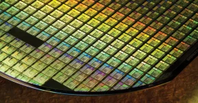
TSMC is running ahead of plan with its top chip factories making the advanced 2 nm chips. These plants expect to start large-scale production in the coming months, freeing up space for next-generation experiments. Reports from Taiwan Economic Daily News suggest behind-the-scenes activity at the Baoshan P2 plant, which appears ready for an incredibly tiny 1.4 nm chip design. Sources claim TSMC achieved a breakthrough with this cutting-edge 1.4 nm process technology. The company already asked suppliers to get equipment ready, planning to build a test production line at their Baoshan location.
The Hsinchu area Fab 20 plant leads the early testing for this super-advanced technology. Industry experts believe the 1.4 nm knowledge will later spread to the nearby P3 and P4 factories when full production begins. These sites originally had assignments to make 2 nm wafers before this shift happened. The company might also test 1.4 nm work at its Fab 25 campus, according to Taiwan business press reports. Four different plants located in Central Taiwan Science Park apparently joined forces on this project.
Market research firm TrendForce predicts the P1 plant could start early test runs by 2027. They expect full production capabilities would follow about a year later. This represents an aggressive timeline for what would become some of the most advanced chip manufacturing technology on earth. The semiconductor industry watches TSMC closely as it pushes the boundaries of what manufacturers can create on silicon wafers. Each smaller process node brings potential improvements in power efficiency and performance.
These developments matter greatly as computing demands grow across artificial intelligence, cloud services, and mobile devices. TSMC stays ahead of competitors through these rapid advancements in manufacturing technology. The leap from current production to 1.4 nm processes would maintain TSMC's leadership position against rival chipmakers. Companies like Apple, AMD, and Nvidia depend on TSMC's ability to deliver cutting-edge manufacturing capabilities for their future products.