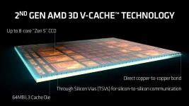
AMD engineers are essentially hacking physical space to make future processors way faster. A fresh research paper reveals plans for stacking L2 cache layers, which builds on the existing tech used for Ryzen and Epyc chips. This design uses vertical silicon vias located right in the center of the stack.
Placing these connections in the middle balances data travel distances. This specific layout prevents the need for extra wire stages, which usually slow things down in flat designs. Shorter wires mean less capacitance, resulting in chips that generate less heat.
Testing shows a stacked one megabyte cache hits a twelve-cycle latency, beating the fourteen cycles seen on standard flat versions. These stacked modules can scale up to four megabytes while maintaining those snappy speeds. Using fewer cycles to fetch data also lets the hardware hit idle states much faster.
Efficiency gains look massive because signals only travel half the usual distance. While this tech is still in the patent phase, it signals a major shift for upcoming silicon. Advanced cache control circuitry manages the flow between the stacked compute and memory layers.