Apple's latest iPhone Air measures just 5.6mm thick, creating significant space constraints for internal components. Engineers initially appeared to relocate all hardware into the device's camera bump area. Recent motherboard design revelations from tipster ShrimpApplePro challenge this assumption. The leaked schematics reveal that Apple positioned only the A19 Pro processor within the camera bump region. The remaining printed circuit board elements must coexist with the battery in the main chassis.
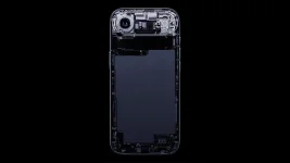
The logic board features an irregular shape that prevents complete placement within the camera bump alone. Apple employs a dual-sided component layout to maximize space efficiency. The C1X 5G modem and N1 wireless networking chip occupy opposite sides of the board. Illustrations from @BasQuxFoo demonstrate how the A19 Pro exclusively occupies the camera bump space. Future iPhone generations may achieve complete logic board integration within the camera cluster, allowing larger batteries and extended device runtime.
The logic board features an irregular shape that prevents complete placement within the camera bump alone. Apple employs a dual-sided component layout to maximize space efficiency. The C1X 5G modem and N1 wireless networking chip occupy opposite sides of the board. Illustrations from @BasQuxFoo demonstrate how the A19 Pro exclusively occupies the camera bump space. Future iPhone generations may achieve complete logic board integration within the camera cluster, allowing larger batteries and extended device runtime.