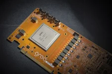
NVIDIA's next Feynman chips might stack LPU units using advanced bonding tech. An expert theory suggests the company could use TSMC's hybrid bonding, similar to AMD's 3D V-Cache, to attach separate LPU dies packed with SRAM onto a main A16 process compute die. This move follows NVIDIA's IP deal with Groq and aims to dominate the AI inference market by combining GPU flexibility with deterministic LPU throughput.
The proposed design would place large SRAM banks on dedicated LPU dies bonded to the Feynman die containing tensor cores and control logic. This approach supposedly saves expensive silicon area since SRAM does not scale well on advanced nodes. TSMC's bonding tech would provide a wide, low-power connection, while backside power delivery on the A16 node could free the front for low-latency vertical links to the stacked memory.
Major challenges include managing heat from stacked high-density components and resolving execution conflicts. LPUs use a fixed order of operations, which clashes with the flexible nature of CUDA kernels designed for hardware abstraction. NVIDIA would need to engineer a deeply optimized LPU-GPU environment, handling explicit memory placement against CUDA's abstractions. Overcoming these hardware and software hurdles is the steep price for inference leadership.