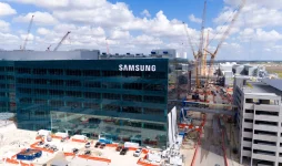
Samsung prepares to establish a $7 billion advanced packaging facility in the United States after securing a significant contract with Tesla. The South Korean semiconductor manufacturer had previously struggled to attract major clients for its foundry operations. Chairman Jay Y. Lee will travel to America to participate in trade discussions between the two nations. The company initially committed $44 billion to US expansion but reduced this amount during economic uncertainty. The Tesla partnership has restored Samsung's confidence in American market investments.
The United States currently lacks high-end chip packaging facilities, while Taiwan Semiconductor Manufacturing Company expects to complete similar operations by 2030. Samsung's proposed facility would position the company competitively against TSMC in the American market. SK Hynix also plans to construct a specialized DRAM manufacturing plant for high-bandwidth memory production targeting NVIDIA. These Korean investments form part of broader negotiations aimed at securing favorable trade agreements. Both companies seek to expand their presence in the lucrative US semiconductor market.
The United States currently lacks high-end chip packaging facilities, while Taiwan Semiconductor Manufacturing Company expects to complete similar operations by 2030. Samsung's proposed facility would position the company competitively against TSMC in the American market. SK Hynix also plans to construct a specialized DRAM manufacturing plant for high-bandwidth memory production targeting NVIDIA. These Korean investments form part of broader negotiations aimed at securing favorable trade agreements. Both companies seek to expand their presence in the lucrative US semiconductor market.