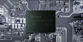
SK Hynix advances memory technology through its ambitious 1c DRAM development program. The company will become the first manufacturer to implement six EUV layers in production processes. This approach surpasses Samsung's recent technological moves in the semiconductor field. The Korean firm expects superior performance across DDR5 and HBM product lines. Market leadership appears achievable through these strategic manufacturing changes.
EUV lithography utilizes a 13.5-nanometer wavelength to create intricate circuit patterns with fewer multi-patterning steps. Previous DRAM manufacturing combined both EUV and DUV layer technologies. SK Hynix will transition completely to six EUV layers for enhanced efficiency. Higher yields and improved profit margins become possible through this shift. Performance gains accompany the manufacturing process improvements.
Consumer memory solutions have not yet adopted 1c DRAM for widespread use. SK Hynix explores applications for future DDR5 products with expanded capacities. The company pursues High-NA EUV integration for long-term development. Next-generation technologies will rely heavily on EUV processes. HBM4 products may showcase the dominant market entry.