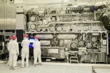
Intel Foundry got ASML's second-generation High-NA EUV lithography machine running at its fab and became the first outfit to move from Low-NA tech to the new hotness for its 14A process node. The TWINSCAN EXE:5200B can crank out 175 wafers per hour stock, but Intel wants to tune it past 200 wafers hourly while hitting overlay precision down to 0.7 nanometers for stacking chip layers.
The company already blasted through over 30,000 wafers in one quarter on the earlier High-NA scanner and cut a specific manufacturing layer from 40 steps down to under 10. Customers got their hands on the 14A development kit and seem hyped about the yield numbers that beat what 18A pulled off at the same stage.
Volume production kicks off in a couple of years, but Intel needs more machines to handle serious foundry capacity since 30k wafers per quarter only covers a handful of clients. The older 18A node sticks around on Low-NA gear to balance output demands.