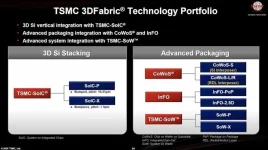
TSMC showed off its packaging tech plans at the Technology Symposium this year. The company works with two main packaging types: Advanced Packaging and System-on-Wafer. CoWoS-S started in 2016 with four HBM stacks joined to N16 compute dies on a small interposer. Today, CoWoS-S holds eight HBM chips with N5 and N4 compute tiles on larger bases. CoWoS-R comes next with better connections and N3-node support.
TSMC plans to launch CoWoS-L around 2027. It will first use large N3-node chiplets, later adding N2-node tiles, multiple I/O dies, and up to twelve HBM3E or HBM4 stacks. The whole package fits under a bigger size limit. Eight HBM stacks once seemed hard to achieve, but they became standard for new AI systems like AMD Instinct MI450X and NVIDIA Vera Rubin.
InFO offers another option with flexible 3D designs. AMD Instinct cards already use the first InFO bridge version. InFO-POP and InFO-2.5D arrive later this year, letting chips stack higher and closer together. These methods help fit more power into one package, moving past flat designs into three dimensions.
TSMC also makes System-on-Wafer products called SoW-P and SoW-X. These grew from special AI chips into a full product line that matches their logic progress. This year brings the first SoIC stacks from N3 to N4, with tiles up to 830 square millimeters and no size limits for top dies. These changes lead toward huge, dense packages that data centers will need soon.