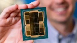
Intel claims its fancy chip glue beats the industry standard for packing silicon. Team Blue published data showing how the EMIB interconnect solution supposedly destroys traditional 2.5D packaging methods. The corporation argues that sticking with standard silicon interposers creates unnecessary cost bloat while hurting production yields. Rivals like TSMC utilize those older setups where wires run through massive silicon slabs called TSVs just to link different dies together.
Intel removes that middle layer completely. Their strategy involves embedding tiny bridges directly inside the substrate exactly where connections need to happen. This specific tech powers heavy hitters like Ponte Vecchio or Sapphire Rapids alongside the upcoming Clearwater Forest lineup. Engineers suggest this approach offers way more flexibility for mixing various compute and memory units without hitting size limits.
Two main versions exist to handle these complex tasks. The 2.5D variant connects logic or bandwidth memory efficiently, while the 3.5D option combines everything with Foveros stacking for monster chips. These tools aim to attract foundry clients who want scalable designs for data centers. Success here relies on the 14A node proving itself capable of American manufacturing dominance.